

New Delhi: India has unveiled an ambitious semiconductor roadmap that seeks to reposition the country from a large-scale chip importer to a strategic pillar in the global electronics supply chain, betting heavily on advanced packaging, compound semiconductors and AI-native chip design rather than attempting a costly race for cutting-edge wafer fabrication dominance.
The push comes at a time when semiconductors have become central to economic competitiveness, defence preparedness, artificial intelligence, electric mobility and digital infrastructure, prompting governments worldwide to secure domestic capabilities amid rising geopolitical fragmentation and supply-chain vulnerabilities.
In the roadmap, titled Future of India’s Semiconductor Industry, prepared by the Niti Aayog’s Frontier Tech Hub, the government lays out a calibrated strategy focused on “becoming indispensable, not imitative” in the global semiconductor ecosystem. According to the report, India should target building a $120-150 billion semiconductor value chain by 2035 while emerging as one of the top three global destination for advanced OSAT (outsourced semiconductor assembly and test) and packaging capabilities.
Finance Minister Nirmala Sitharaman framed the roadmap as a strategic declaration of intent. “Semiconductors are the foundational infrastructure of the 21st century. They power AI, electric mobility, telecommunications, defence systems, healthcare technology, digital public infrastructure, and advanced manufacturing,” she said, adding that the roadmap focuses on advanced packaging, compound semiconductors, wide-bandgap materials, and AI-native chip design.
Electronics and IT Minister Ashwini Vaishnaw said the government’s priority under India Semiconductor Mission 2.0 (ISM 2.0)would be to build the “full ecosystem — design, talent, materials, equipment, fabs and advanced packaging” to make India a dependable node in global supply chains. He described semiconductor development as a “20-year journey” central to India’s “technological sovereignty and strategic autonomy”.
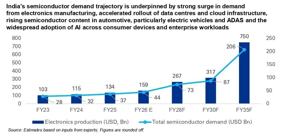
The urgency is driven by India’s overwhelming import dependence. According to the Niti report, nearly 90-95% of India’s semiconductor demand is currently met through imports, exposing sectors ranging from automobiles and telecom to defence and healthcare to supply disruptions. The report estimates India cumulatively spent almost $150 billion importing semiconductor products between FY17 and FY25, with annual import costs potentially rising to $240 billion by 2035 if current trends continue.
“One of the biggest strategic risks to Viksit Bharat is a growing dependence on imported black-box technologies. For India to become a developed nation, technological sovereignty is foundational. And that sovereignty must begin at the infrastructure layer,” the report said in a message by Ashok Kumar Lahiri, Vice Chairman, Niti Aayog. “Semiconductors sit at the heart of this foundation, powering everything from AI, defence and manufacturing to mobility, energy systems, communications and citizen services.”
Packaging Over Fabs
Rather than directly confronting established leaders such as Taiwan and South Korea in leading-edge wafer fabrication, the roadmap advocates a differentiated strategy focused on mature-node manufacturing, advanced packaging and compound semiconductors including Silicon Carbide (SiC) and Gallium Nitride (GaN).
“Winning the semiconductor race will not be easy if India continues to run the existing race; instead, it should shift gears and target becoming the ecosystem player that the global semiconductor industry cannot run without,” the report said. “This requires India to pivot away from the catch-up game in the foundry race and focus on winning the ‘More-than-Moore’ era, where advanced packaging, system integration and manufacturing scale matter as much as transistor nodes.”
The report projects the global semiconductor market will exceed $1.5 trillion by 2035, while India’s semiconductor demand could surpass $200 billion during the same period, fuelled by AI computing, data centres, electric vehicles, telecom infrastructure and industrial automation.
India already possesses structural advantages in semiconductor design. The report highlights that Indian professionals account for nearly one-fifth of the global semiconductor design workforce, giving the country a strong base in engineering and software integration. The roadmap proposes leveraging this talent pool to create more than 100 breakthrough semiconductor intellectual properties by 2035.
The roadmap also identifies advanced packaging as India’s most realistic opportunity to gain global scale. It recommends establishing a National Centre for Advanced Packaging, scaling capabilities in 2.5D and 3D integration, chiplet assembly, fan-out wafer-level packaging and heterogeneous integration technologies increasingly critical to AI and high-performance computing systems.
“Future value in semiconductors will increasingly come from advanced packaging, chiplets, heterogeneous integration, compound semiconductors, wide-bandgap materials such as SiC and GaN, specialised chips for AI and 5G/6G and system-level design,” said Debjani Ghosh, Distinguished Fellow, Niti Aayog. “The challenge is not merely to participate in the global ecosystem, but to become indispensable to it.”
The strategy aligns closely with the government’s expanding India Semiconductor Mission. The roadmap estimates the country would require $135-180 billion in semiconductor investments over the next decade across fabrication, packaging, materials and design infrastructure. It recommends that the government commit at least one-third of the required capital to de-risk projects and crowd in private investment.

Race Against Time
The roadmap repeatedly underlines that India’s semiconductor ambitions face formidable execution risks, including technological complexity, talent shortages, infrastructure bottlenecks, long gestation periods and high capital intensity.
Building advanced fabs remains among the world’s most expensive industrial undertakings. According to the report, leading-edge 3 nm fabrication facilities globally cost more than $15 billion, while even analog fabs typically require investments exceeding $5 billion. The report says semiconductor manufacturing also demands uninterrupted electricity, ultra-pure water systems and highly specialised engineering talent that India currently lacks at scale.
“Semiconductors represent one of the most consequential industrial opportunities of the coming decade for India,” the report said. “While the cost of inaction is clear — rising import dependence, strategic vulnerability and lost value creation—the opportunity is equally profound.”
The roadmap calls for a coordinated national effort spanning policy, research, education and global partnerships. It proposes creating National Semiconductor Zones with integrated utilities, specialised fab academies, sovereign access to electronic design automation tools, dedicated export financing windows and structured partnerships with countries including the US, Japan, the European Union and South Korea.
It also advocates using AI to compress semiconductor design cycles and democratise access to advanced chip engineering. “AI solutions are helping design firms navigate the intricate design process with remarkable precision and reduce design and R&D costs, while improving time to market performance,” the report said. “By leveraging its deep talent pool in AI, India can excel in developing custom design solutions tailored to domestic use cases.”
Lahiri warned that semiconductor dependence increasingly carries strategic consequences beyond economics. “One of the biggest risks India carries today is its dependence on technology controlled by others. Sovereignty in this century will begin with the infrastructure layer, and semiconductor leadership is part of that foundation,” he said.
For policymakers, the roadmap marks a clear shift in India’s semiconductor strategy — from chasing prestige manufacturing projects to building leverage in high-growth segments where the global industry itself is being redefined by AI, advanced packaging and system integration. The success of that strategy, however, will depend less on ambition and more on whether India can sustain policy consistency, capital commitment and industrial execution over the next decade.